| dc.contributor.author | Farag, Heba | |
| dc.date.accessioned | 2023-01-04 15:54:21 (GMT) | |
| dc.date.available | 2023-01-04 15:54:21 (GMT) | |
| dc.date.issued | 2023-01-04 | |
| dc.date.submitted | 2022-12-21 | |
| dc.identifier.uri | http://hdl.handle.net/10012/19023 | |
| dc.description.abstract | Non-destructive testing (NDT) is the method where an object or materials are being
tested for any type of damage or features without harming the object during the process.
There are different NDT techniques; in this thesis the main focus is to explore the feasibility
of using eddy current (EC) non-destructive testing technique to detect different types of
flaws in metallic parts. One of the contributions in this project is to develop different
models to design an EC probe that is sensitive to detect small flaw sizes in parts made
by additive manufacturing. Additive manufacturing (AM) is the process where an object
is created by layering materials based on three dimensional (3D) Computer-Aided Design
(CAD) data. In this thesis, the main focus are the products created by laser powder
bed fusion process (LPBF) which is one of the metal AM technologies. Defects such as
pores and cracks will be created within the parts because of, but not limited to the unmelted
powder or the excessive material vaporization during laser-material interaction. The
existence of these defects will affect the quality of parts therefore, NDT should be done on
these parts for early detection of defects. Eddy current probes have been designed based on
modelling developed to detect subsurface defects in parts made by the LPBF technology.
Several samples made of stainless steel (316L) and titanium (Ti64) were considered for
the detection process to explore the probe response while testing different materials with
different conductivity and permeability. Artificial defects were embedded inside the parts
at different depths, with different geometries and sizes as well. The probes operate at
a wide frequency range for the purpose of increasing the standard depth of penetration
of the eddy currents inside the material which, increase the probes, sensitivity to detect
subsurface flaws. Experiments were carried out to further test the performance of the
designed probes to detect flaws embedded inside parts made by AM.
Some of the challenges in testing parts made by AM are the surface roughness and the
effect of edges. The problem of edge effect phenomena is a major problem when it comes
to testing small samples. The edge of the small sample will create a signal that is similar
to the one obtained from a crack. The small diameter of the probe coil and the tip added
to it helps distinguishing between the actual defect signal and the signal produced by the
test piece edge. Another contribution is that the EC probe is designed in a way that can
overcome the problem of surface roughness and the unwanted resultant signal produced by
rough surface by adding a coating layer made of thin paper to the bottom of the probe;
some of the experimental findings and contributions are listed below:
Subsurface notches that simulate subsurface cracks with different sizes in the range of
(0.07 mm-0.4 mm) and subsurface blind holes with different diameters in the range of (0.2
mm-0.5 mm) embedded inside plates made of stainless steel and titanium materials have been detected successfully. The plates sizes are 50 mm×50 mm. FEM models with the
same parameters were created in ANSYS Maxwell to validate the experimental results.
Multiple probes with different parameters such as number of turns, length, inner and
outer diameter were designed to investigate the effect of each parameter on the sensitivity
of the probe to detect small size defects. Core tip analysis for focusing the magnetic field
were done. Different tip shapes of the core with different geometries were considered to
increase the detectability of the probe to subsurface defects. Optimization for the designed
probe was conducted to determine the optimal probe parameters such as length, inner and
outer diameter that gives the best values for the magnetic field. Shields with different
thickness were added around the coils to increase and focus the eddy current distribution
under the probes coils. Amplification circuits were attached to the probe coil winding to
amplify the detected defect signal since the measured detected signals are in millivolts. In
conclusion, it is clear that the eddy current testing technique has a potential to be used to
inspect parts made by AM. | en |
| dc.language.iso | en | en |
| dc.publisher | University of Waterloo | en |
| dc.subject | absolute probe | en |
| dc.subject | additive manufacturing | en |
| dc.subject | defects | en |
| dc.subject | eddy current | en |
| dc.subject | magnetic coil | en |
| dc.subject | magnetic sensors | en |
| dc.subject | non-destructive testing | en |
| dc.subject | sensor design | en |
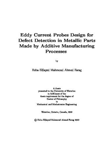
| dc.title | Eddy Current Probes Design for Defect Detection in Metallic Parts Made by Additive Manufacturing Processes | en |
| dc.type | Doctoral Thesis | en |
| dc.pending | false | |
| uws-etd.degree.department | Mechanical and Mechatronics Engineering | en |
| uws-etd.degree.discipline | Mechanical Engineering | en |
| uws-etd.degree.grantor | University of Waterloo | en |
| uws-etd.degree | Doctor of Philosophy | en |
| uws-etd.embargo.terms | 0 | en |
| uws.contributor.advisor | Khamesee, Behrad | |
| uws.contributor.advisor | Toyserkani, Ehsan | |
| uws.contributor.affiliation1 | Faculty of Engineering | en |
| uws.published.city | Waterloo | en |
| uws.published.country | Canada | en |
| uws.published.province | Ontario | en |
| uws.typeOfResource | Text | en |
| uws.peerReviewStatus | Unreviewed | en |
| uws.scholarLevel | Graduate | en |

